
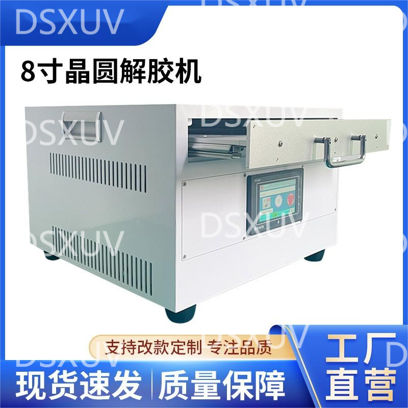
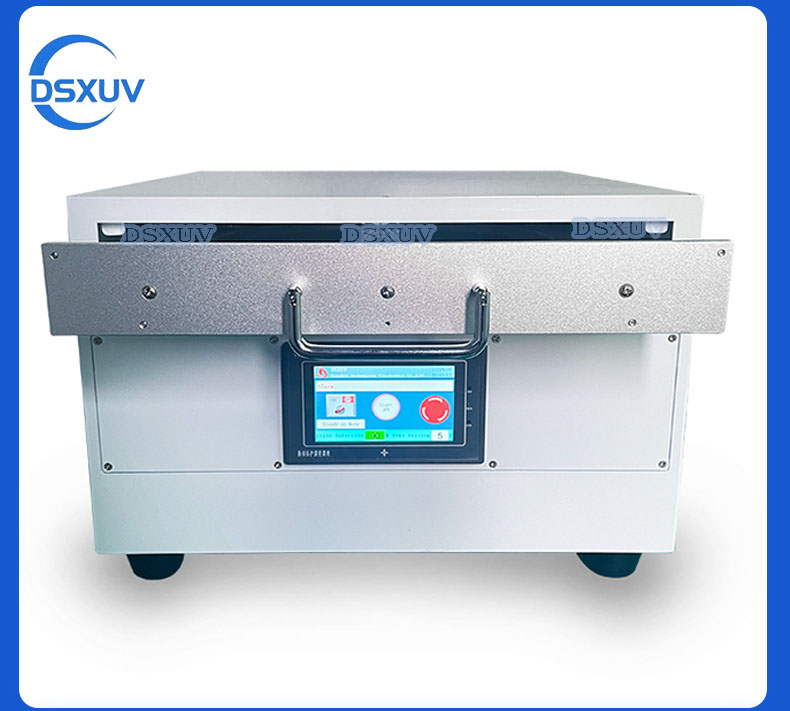

| Model Model |
DSXUVtape8 | Manufacturer Manufacturer |
Shenzhen Deshengxing Electronics Co., Ltd. Shenzhen Desheng Xing Electronics Co., Ltd. |
| Dimensions overall size |
L459 × W416.5 × H270 mm | Compatible sizes Compatibility size |
8 inches and under 8″ and above |
| Cooling method A cool method |
Air-cooled Air-cooled |
Power Input DSXI Input power |
100–240 V AC, 50–60 Hz |
| Total power Total power |
1000W | Wavelength Wavelength |
365 nm UV LED |
| Lumen space XL | L330mm × W330mm × H13mm | Illuminance Tlluminance |
>600 mW/cm² |
| Material/Weight Material/Weight |
White sheet metal / 30 kg White sheet metal / 30 kg |
Display/Language Display/language |
Touchscreen English Touch screen (English) |
| Features Function |
Adjustable time and illuminance Adjustable time and brightness |
Irradiation direction | From the bottom up From the bottom up |
| Quality Assurance / Extended Warranty / Peace of Mind |
Principle of the UV de-gelling machine:
In the semiconductor chip manufacturing process, prior to die cutting, the wafer is secured to a frame using a die-cutting adhesive film. Once the die-cutting process is complete, the adhesive film is exposed to UV light to cure and harden it, thereby reducing its tackiness and ensuring the smooth progression of subsequent packaging operations.
In other words, UV tape has very high adhesive strength and holds the wafer firmly in place during the wafer grinding or dicing processes. When exposed to ultraviolet light, the adhesive strength decreases. Consequently, after exposure to ultraviolet light, the wafer or chip can be easily peeled off the tape.
UV de-bonding machines address the de-bonding stage in the cutting processes for wafers, glass and ceramics. Their applications are currently not limited to the semiconductor packaging industry; they are also suitable for the removal of UV films from semiconductor materials used in optical lenses, LEDs, ICs, semiconductors, printed circuit boards and portable hard drives.
UV de-resin machines in the current state of the art predominantly utilise UV mercury lamps; however, as mercury lamp light sources generate a high level of heat, they are prone to damaging heat-sensitive materials. Furthermore, they are inefficient and make it difficult to accurately control quality standards, rendering them unsuitable for irradiating high-precision components such as chips.
Shenzhen Deshengxing Electronics Co., Ltd. utilises an environmentally friendly, low-temperature LED UV light source for its debonding machine, which effortlessly completes the UV film debonding process without damaging the wafers, thereby fully meeting production requirements.
Product features:
◆ Compact design, suitable for full-chip illumination of 4-, 6- and 8-inch chips
◆ Adjustable time and brightness; touchscreen operation; simple and convenient
◆ Bottom-up illumination, making it easy to position wafers
◆LED cold-light sources are environmentally friendly products characterised by low temperature, uniform exposure and a compact design, whilst consuming minimal energy; they are ideal for the semiconductor industry, and the low temperature causes no damage to heat-sensitive materials.
◆ The service life is more than 10 times longer than that of standard mercury lamps, with a continuous service life of 15,000–30,000 hours.
◆ Zero maintenance costs; no need to replace the light source components during long-term operation
◆ Enclosed light source design, with no UV leakage, and harmless to humans
◆ The adhesive comes off quickly; it can be removed in a matter of seconds
◆ Backwards compatibility with smaller sizes is supported