
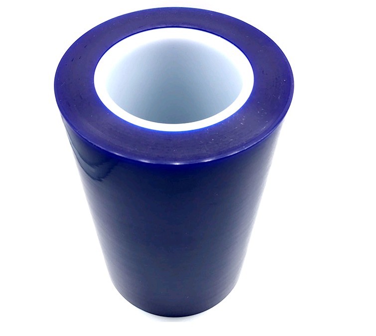
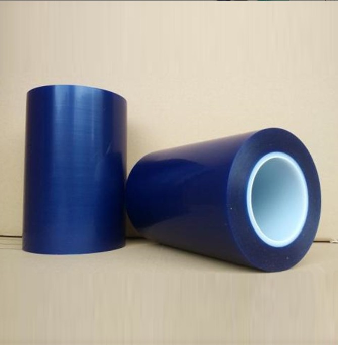
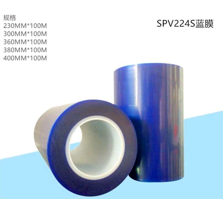
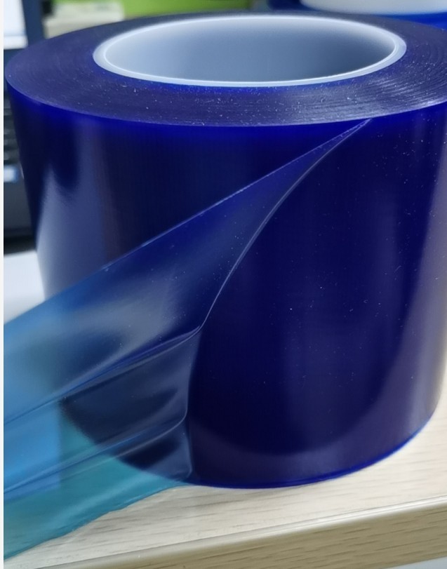
Nitto Blue FilmProduct description:
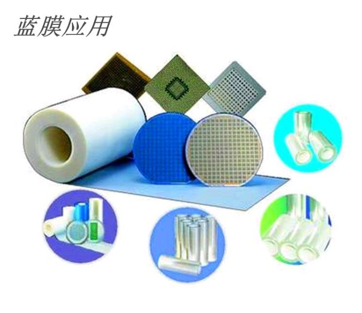
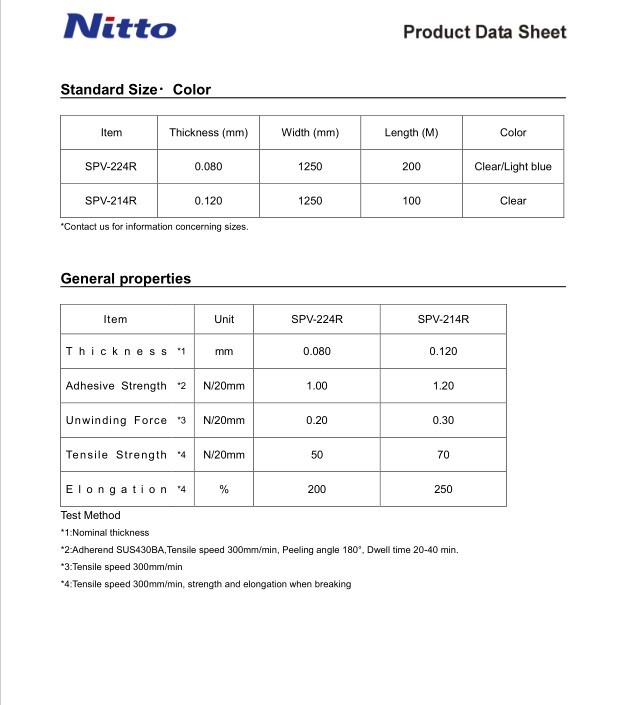
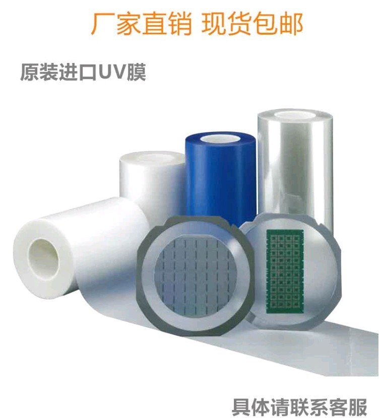
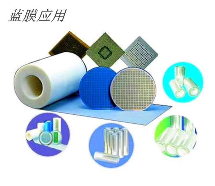
1. Blue protective tape is used in semiconductor wafer fabs or packaging plants during the back-side grinding, dicing and thinning processes.
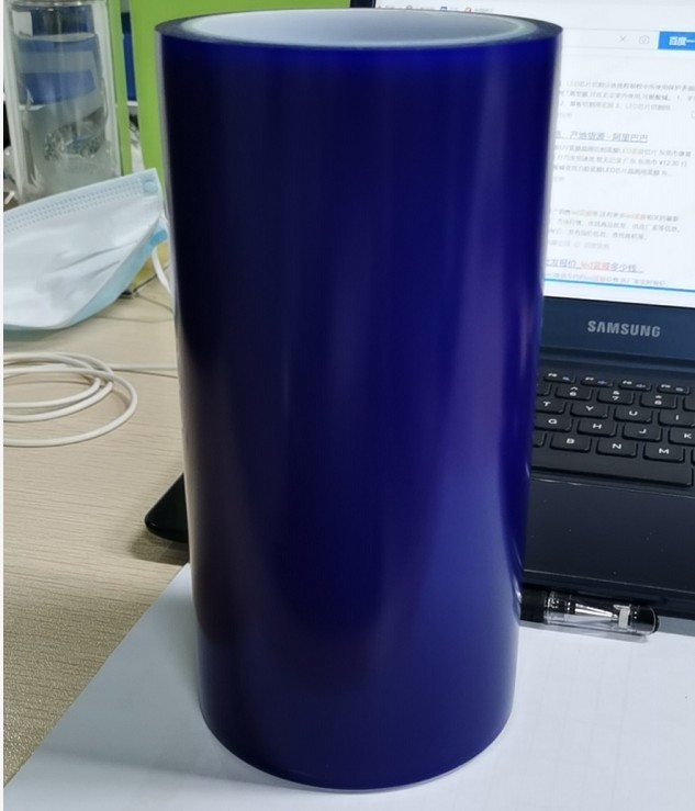
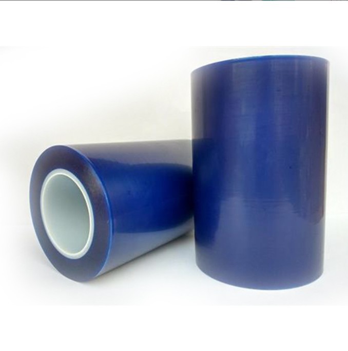
Common sizes for LED die attachment are 180 mm × 100, 200 mm × 100, 230 mm × 100 and 280 mm × 100.
II. Purpose:
1. Semiconductor silicon wafers — blue film for cutting, UV film for cutting, protective film with release liner
2. Semiconductor silicon wafers — thinning, back-grinding
3. Semiconductor silicon wafers — film that can be torn by hand after thinning
4. Semiconductor silicon wafers — Flip-chip film
5. Semiconductor silicon wafers — thermal release film, UV film
6. Blue protective tape is used as surface protection tape during the back-side polishing process of silicon wafers in IC/semiconductor manufacturing.
A protective film for the circuit surface during the back-grinding of semiconductor silicon wafers (IC/semiconductor process).
A film used during the polishing of semiconductor silicon wafers.
Country of origin: Original manufacturing sites in the United States, Japan, Taiwan and elsewhere.