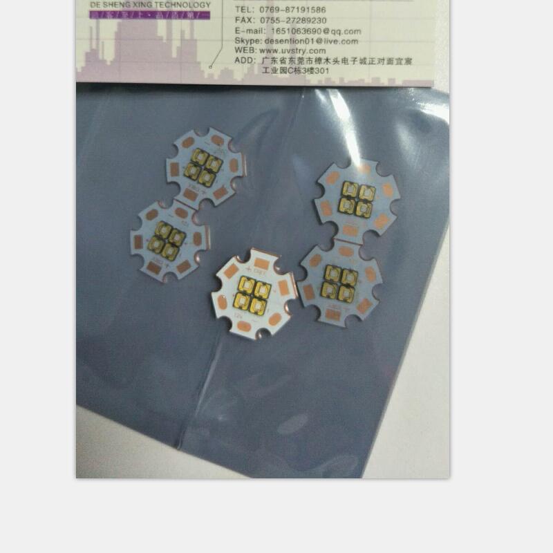
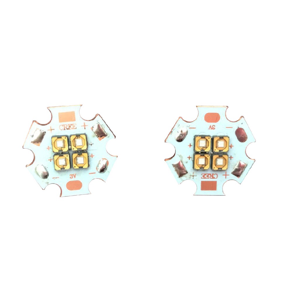
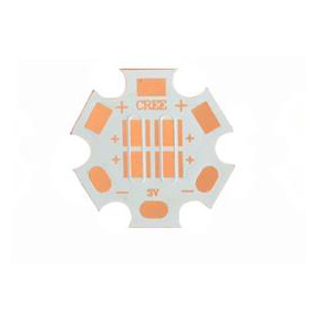
CUN6GF1A 365nm 4-cell 12V copper plate specifications: 20mm × 1.5mm
CUN6GF1A 365 nm 4 strings, 12 V Copper plate dimensions: 20 mm × 1.5 mm
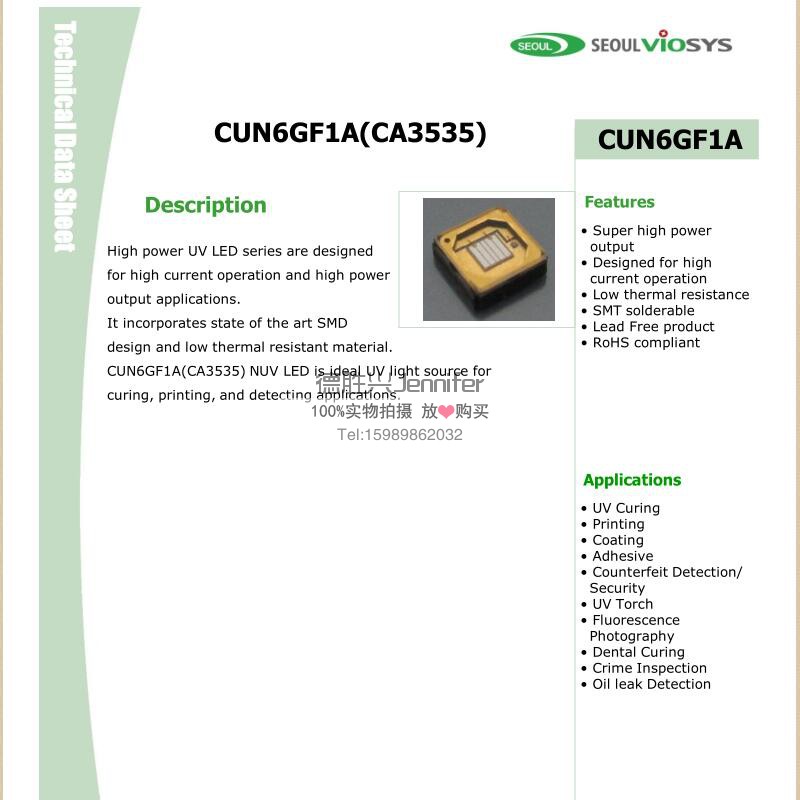
Specifications for a single UV LED:
Model: CUN6GF1A
Country of origin: Imported directly from South Korea
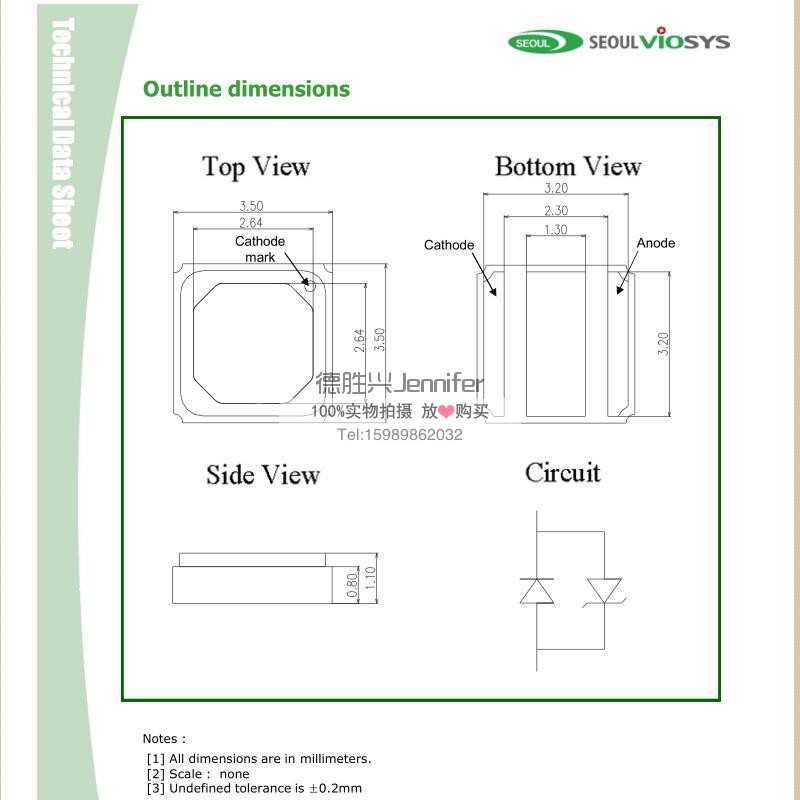
Package dimensions: 3.5 × 3.5 mm
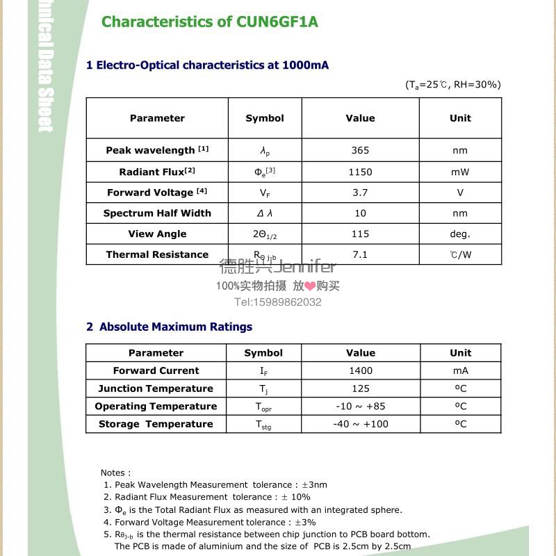
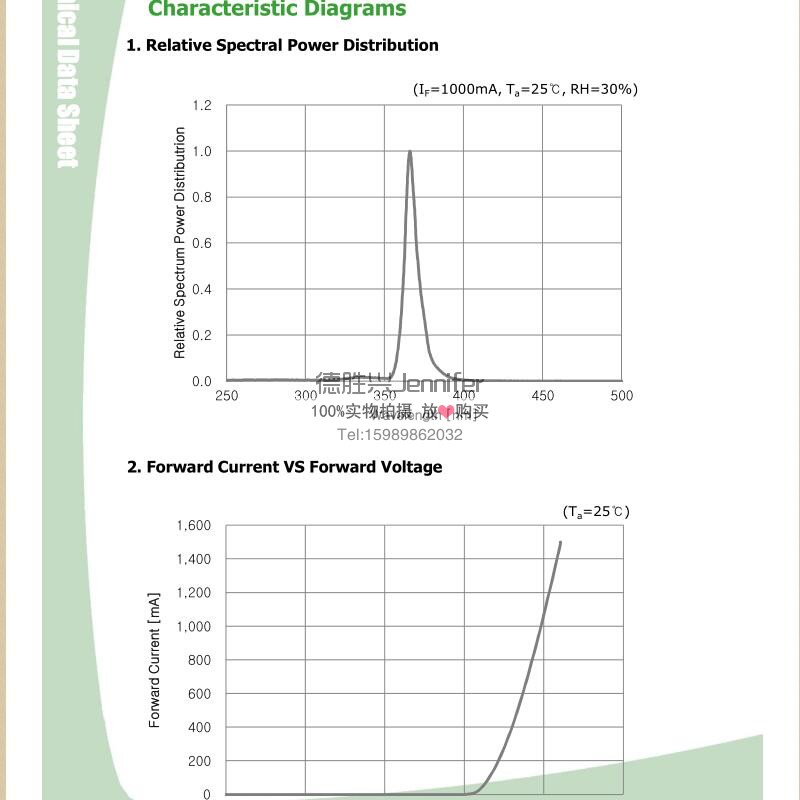
Peak wavelength: 365 nm
Radiated power: greater than 1150 mW
Power consumption: 5W
Voltage: 3.7V
Current: 1400 mA
Beam angle: 115 degrees
Encapsulation material: flat-edged quartz glass window
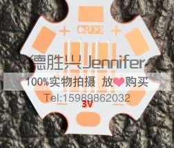
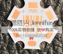
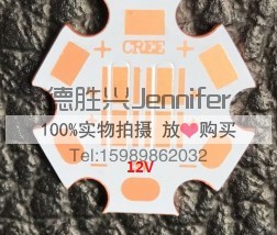
Copper plate specifications: 20 mm diameter × 1.5 mm thick ——Click to view other copper plate specifications
Purpose:
It is most commonly used in the fields of UV curing and bonding, such as the curing of UV adhesives and UV inks. The corresponding equipment includes UV LED point light sources, UV LED line light sources and UV LED area light sources.
Penetrant testing, fluorescent penetrant testing.
Biopolymerisation, fluorescence observation.
Detection of air-conditioning refrigerant leaks.
Detection of engine oil leaks.
Criminal Investigation: Examination of fingerprints and bloodstains.
Fluorescence observation of ore.
Oil stain cleaning and inspection.
Fluorescent non-destructive testing: fluorescent penetrant testing and fluorescent magnetic particle testing for steel, non-ferrous metals, motor vehicles, aircraft and other applications.
Contamination checks: electronic components, motherboards, dust checks, LCD panels, and checks on personnel entering the cleanroom.
Leak detection: Checking for oil leaks in hydraulic machinery, fluid reservoirs, piping, etc.; using fluorescent dye to detect water leaks.
Degreasing and cleaning verification: Verification of degreasing and cleaning in the food industry, kitchens, cookware and tableware.
Other industrial applications:
Linear light curing for microelectronics, liquid crystal displays, printed circuit boards, optical communications, optics, etc.;
Curing of UV varnish on high-end furniture;
Print anti-counterfeiting verification;
Spray-coating and curing of craft items;
Sealing of the encapsulation port on a TFT-LCD panel.
Curing of the sides of capacitive touchscreens; curing of the edge seals
Side curing of LCD liquid-gel lamination
Side-curing of water-based adhesive lamination for mobile phone screen refurbishment
Edge Sealing and Curing of LED, LCD and OLED Screens
Linear curing, gap curing, gap bonding
In smartphone apps
1. Bonding the mobile phone screen to the phone’s bezel
2. Bonding of mobile phone casings
3. Adhesive fixing of the side buttons
4. Positioning the camera window
5. Affixing the logo
6. The cover of the sound chamber in the smartphone
7. Between the FPC antenna and the casing of a smartphone
8. On the camera module, between the holder and the FPC (the area where the FPC is bent)
9. Secure the wiring for the flat motor on the mobile phone.
10. Securing the mobile phone’s motherboard
Microelectronics Industry – UV Curing Applications
1. Mobile phone component assembly (camera lenses, earpieces, microphones, casings, LCD modules, touchscreen coatings, etc.)
2. Hard disk head assembly (gold wire bonding, bearings, coils, chip bonding, etc.)
3. DVD players/digital cameras (lenses, lens bonding, circuit board reinforcement)
4. Assembly of motors and components (wiring, securing coils, securing coil ends, bonding PTC/NTC components, securing the protective transformer core)
5. Semiconductor chips (moisture-proof protective coating, wafer masking, wafer contamination inspection, UV tape exposure, wafer polishing inspection)
6. Sensor manufacturing (gas sensors, photoelectric sensors, fibre-optic sensors, optical encoders, etc.)
Applications of UV LED Curing in the PCB Industry
1. Securing components (capacitors, inductors, various plug-in components, screws, chips, etc.)
2. Moisture-proof potting and protection of core circuits and chips; anti-oxidation coating protection
3. Conformal (corner) coating for printed circuit boards
4. Earth wire, jumper wire, coil fixing
5. Through-hole mask for wave soldering
Applications of UV LED Curing in Medical Devices
UV adhesive bonding facilitates the cost-effective, automated assembly of medical devices. Today, advanced LED UV light source systems—capable of curing solvent-free UV adhesives in a matter of seconds—combined with dispensing systems, provide an effective and economical method for achieving consistent and repeatable bonds in the medical device assembly process.
The optimisation and control of UV light sources are crucial for the manufacture of reliable medical devices. The use of UV-curable adhesives offers numerous advantages, such as lower energy requirements, reduced curing time and space, increased productivity, and greater ease of automation.
UV adhesives are generally used to bond and seal medical devices, which require exceptionally high quality and reliability. UV adhesives are typically used in the assembly of medical devices, for example, where it is necessary to bond: 1) different materials (or materials with differing mechanical properties); 2) materials that are not thick enough to allow the use of welding methods; and 3) pre-manufactured sub-assemblies.
1. Anaesthetic mask 2. Syringe 3. Infusion tube 4. Intravenous infusion set 5. Vascular implant accessories 6. Endoscope 7. Arterial positioning device 8. Tubular drainage device 9. Tracheal tube 10. Blood oxygenator 11. Hearing aid
12. Detection, monitoring and imaging equipment 13. Biochips 14. Bonding of PVC and thermoplastics (polycarbonate and ABS)
Optical Industry – ST-UV LED Light-Curing Applications
1. Optical component assembly (lens assemblies, prisms, optical engine assemblies)
2. Assembly of imaging equipment (microscopes, endoscopes, infrared devices, night-vision devices, probes, etc.)
Applications of UV LED Curing in the Optical Communications Industry
1. Passive components (Wavelength Division Multiplexers (WDM), Arrayed Waveguide Grating (AWG), optical splitters, optical isolators, optical couplers, etc.), bonding or potting of various glass-encapsulated structures, and the mounting of micro-components.
2. Active devices (coaxial devices such as TOSA, ROSA and BOSA; VCSELs; laser collimators, etc.), particularly low-cost, miniaturised plastic packaging structures for FTTX applications
3. Optical fibre cables (outer coating, marking, bonding, fibre-optic gyroscopes)
Research and Academic Institutions – ST-UVLED Light-Curing Applications
1. Polymer chemistry (nanocoatings, light-curing resins, photosensitisers, monomers, UV inks, etc.)
2. Medical polymer materials (medical plastics, catheters), microbiology
3. Photochemistry (photocatalysis, photoexcitation, photosynthesis, etc.)
4. Semiconductors (photo-accelerated etching, cutting, UV-curable tape, etc.)