UV-curing LED chip packaging technology
UVA LED packaging technology: UVA LEDs are generally used for curing applications. Let’s discuss this today.UVA LEDPackaging technology
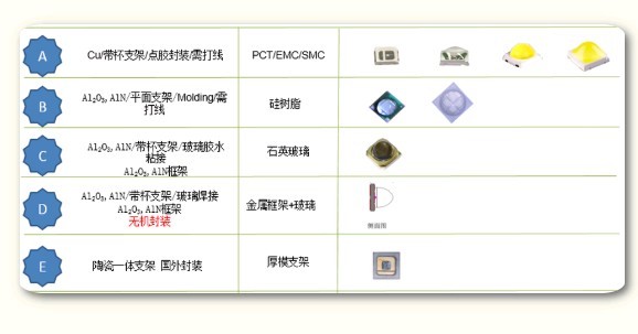
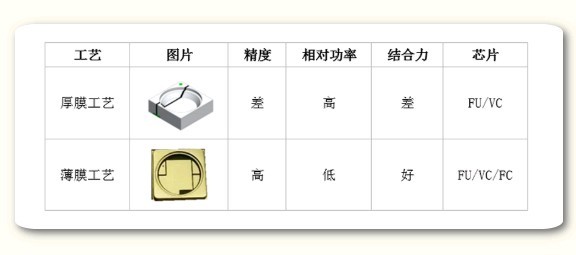
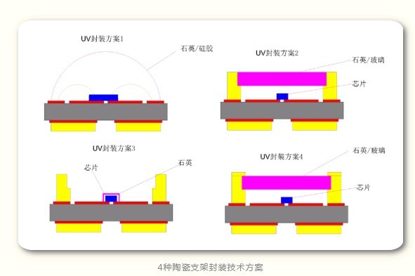
This section primarily covers SMD packaging types with a wide range of applications. Currently, common SMD packaging types can be broadly categorised into the five main categories shown in the figure below: PCT/MEC/SMC, inorganic packaging, … Among these, UV LED products with a power rating of 1W or more primarily utilise ceramic packaging; the ceramic substrates used are generally classified into two main types: thin-film ceramic substrates and thick-film ceramic substrates. At present, ceramic stents produced domestically are primarily manufactured using thin-film processes, whilst those produced overseas are mainly manufactured using thick-film processes. Option 1: Ceramic with Moding encapsulation: Option 2: Ceramic and glass encapsulation: Generally, this can be effectively remedied by employing a secondary optical seal, which can further enhance performance. Option 3: Thick-film packaging: Option 4: Inorganic encapsulation: In the next article, Zixin will continue to share its optoelectronic technology solutions for UVA modules.